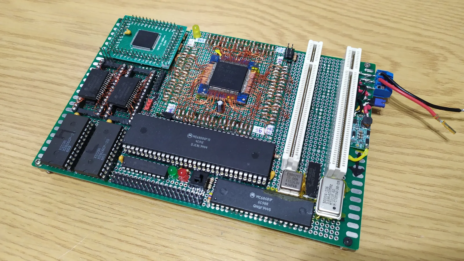
Homebrew 68000 computer with a PCI bus
There might be a situation in which none of the devices lower the DEVSEL#. This means that the address is not covered by any of the cards. This results in an error called "Master Abort", which the operating system shoul…
以下正文同步自 Hacker News 最新,版权归原站所有,已转换为易读排版。
There might be a situation in which none of the devices lower the DEVSEL#. This means that the address is not covered by any of the cards. This results in an error called "Master Abort", which the operating system should handle. Additionally, there may be situations in which the target device does not support burst cycles. The target can abort the transaction by lowering a special signal named STOP#. One data item is transferred and then the transaction ends. To transfer more data, the initiator must repeat the cycle.
Read transactions are similar to this one. The only difference is that there is one enforced wait state after the address phase. This prevents situations in which two devices try to drive the AD bus at the same time when the directions switch. The initiator writes the address onto the AD bus, releases it, waits one cycle and starts a normal data transaction.
I skipped a lot of information, including more explanations of wait states, timeouts (e.g., master aborts), signals (e.g., STOP#), arbitration and more to simplify this brief introduction to the PCI bus. If you want to know more, I recommend reading some literature about it.
From the perspective of software, the PCI is divided into three different accessible spaces:
These spaces are accessed by the C/BE# bus value (command) in the first cycle. It can be: Configuration read/write, memory read/write or I/O read/write. For the configuration space, the desired card is selected by a special signal - IDSEL, which is unique to each PCI slot.
The PCI bus is designed to be little-endian. The value 0xAABBCCDD is stored in memory as follows:
However, on big-endian CPUs, such as the Motorola 68000, the same value stored in memory looks like this:
This becomes problematic when trying to interface the PCI bus with such CPUs. To correctly address bytes or read 16- or 32-bit registers, we need to swap bytes in software or hardware.
There are two techniques we can use for that. We can either preserve the value or the address. The first technique is essentially swapping bytes on the data bus in hardware, ensuring that the 16- or 32-bit number remains unchanged. If the code requests 0xDEADBEEF, the CPU receives 0xDEADBEEF exactly. The issue with this solution is that accessing data in smaller sizes is not straightforward (addressing causes bytes to get swapped). In the second method, we cross the bus so that byte 0 goes to address 0, byte 1 goes to address 1 and so on. We don't care if larger values get scrambled, because we want to preserve the accessed address.
So, value preserving is used when reading or writing a big 32-bit hardware register (like a BAR register) and location preserving is used when writing an array of sequential bytes, like a C string (char*) or a continuous buffer of VGA pixels. With this second method, you get the array to land left to right, exactly as you typed it. Keep this in mind, as I used both methods in the project.
One last thing I would like to mention is PCI interrupts. Each PCI slot has 4 interrupt pins: INTA#, INTB#, INTC# and INTD#. Why four? The PCI specifications allow one PCI device to behave like multiple devices, up to eight. These "subdevices" are called PCI functions. Each function has its own configuration space and registers. Multiple interrupt lines allow interrupts to be spread out onto different potential CPU interrupt lines. Additionally, single-function devices must use the first line INTA#. These interrupt pins are simple: they are standard active-low interrupt pins. They are typically shared; for example, each INTx# pin is connected to other INTx# pins on the board and routed directly to a CPU interrupt line. Shared interrupts are common in PCI.
Once again, I skipped a lot of information about PCI. I explained the basics; probably enough to understand the challenges of implementation. You can find sources and more information here:
After this rather extended introduction, I will now move on to the main topic of this page: the Motorola 68000 homebrew computer with a PCI bus. The idea for this computer actually came to me by coincidence. I received a lot of electronics scrap from my friend Shadowdestroyer777 (huge thanks!). This included an industrial board with a Motorola 68000 CPU, as well as two older broken motherboards (Socket 7 era) for parts. I desoldered the components from the industrial board and one of the broken boards, including the expansion slots, socket, etc. (This was shortly after I had finished working on the experimental FPGA PCI card). The parts from all this work ended up on my desk. One evening, while looking at the desoldered PCI slots, the Motorola 68000 CPU and a prototype board that I had also bought a short time ago, I suddenly thought: "What if I built a 68000 homebrew with PCI on a prototype board?" - and that's how the idea was born.
I took this photo literally when the idea struck!
The prototype board I had was 12x18 cm. At this point, I didn't know which other parts I would use, so I started checking my drawers to see what I had. After searching, checking and selecting, I decided to use the following parts:
I also had a 10 MHz crystal oscillator, which I decided to use as the main clock for everything, including the PCI bus. The idea was to run the PCI bus at the same frequency as the CPU to make it easier to design the logic (FPGA). As I mentioned in the chapter about PCI, the bus is permitted to run at less than the standard 33 MHz. I can also say in advance that the oscillator I used turned out to be faulty. Ultimately, I had to replace it with a 20 MHz oscillator and squeeze in an extra 74163 (4-bit counter) to divide the frequency by two (I didn't have any other 10 MHz oscillators).
There were few challenges because of the parts I had selected:
正文由 探How 从来源站点 RSS 同步,内容未经改写;遇到排版缺失或需要图片、视频时请以原文为准。