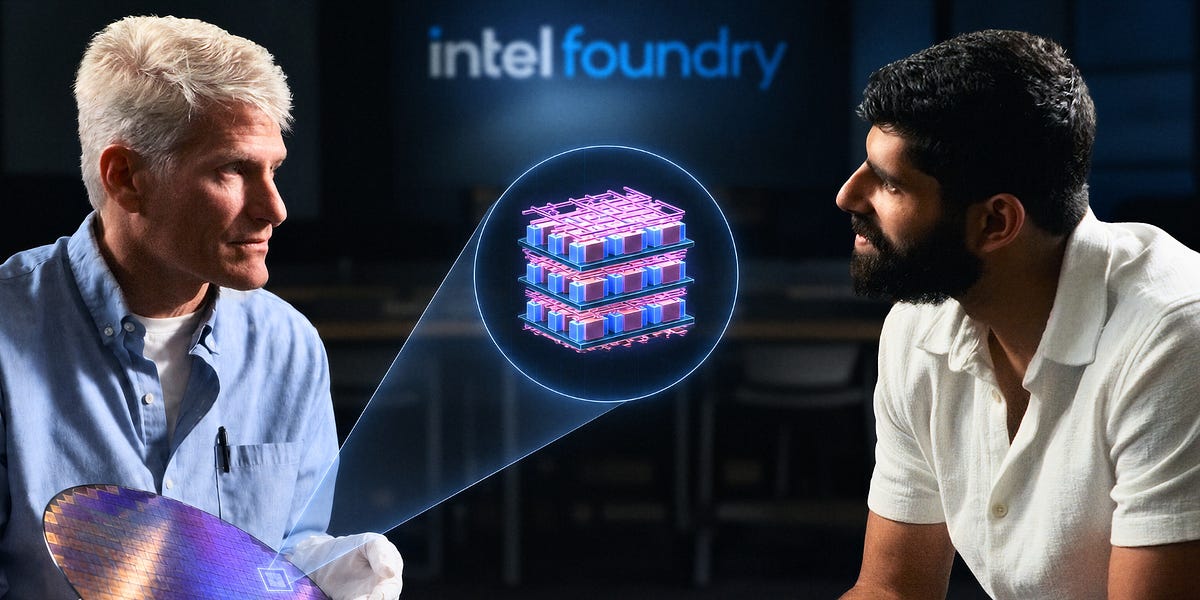
Intel tour by Dwarkesh: What will computer chips look like in 2045?
What will computer chips look like in 2045?
以下正文同步自 Hacker News 最新,版权归原站所有,已转换为易读排版。
Playback speed
×
Share post
Share post at current time
Share from 0:00
0:00
/
20
1
What will computer chips look like in 2045?
What I learned from touring Intel’s most advanced fab and talking to its leadership.
Dwarkesh Patel
Oct 22, 2026
20
1
Share
Transcript
I spent two days touring Intel’s most advanced fab and talking to its technical leadership to understand what the chips of the future will look like.
A lot of what’s coming next – gate-all-around transistors, backside power, CFET, hybrid bonding – is hard to follow without actually seeing it, so we made all the awesome animated explainers that I wish I had while I was prepping.
I also asked Intel’s leadership how the semiconductor industry will cope with the enormous shock in demand from AI.
AI compute has grown 3x a year for the last decade, but according to Intel’s CTO, Intel could only double leading-edge wafer production with today’s global stock of chipmaking tools.
What kinds of tricks can foundries pull to extend this crossover point where demand surges way ahead of supply?
This was a totally new format for us - hope you enjoy!
I also made flashcards for the concepts I had to learn to prep for this episode here.
Watch on YouTube, Apple Podcasts or Spotify.
WorkOS helps you do business with enterprises. It gives you access to all the features most commonly required by enterprises: SSO, SCIM, RBAC, audit logs, and more. It’s easy to plug these features in — it only takes a few lines of code — and WorkOS is releasing new functionality all the time, including things like auth for agents. If you want to join the 3,000+ companies that rely on WorkOS, go to workos.com
Jane Street built a powerful tool called magic-trace to help analyze and debug their trading systems. It only exists because one engineer noticed a feature on Intel chips called Processor Trace and thought it’d be valuable to build on top of. Now, traders and developers across Jane Street use magic-trace every single day! If you want to be trusted to pursue the ideas you think matter most, Jane Street is hiring. Go to janestreet.com/dwarkesh
Antithesis’ testing platform lets you perfectly reproduce every single bug you find. That’s because it runs on a fully deterministic computer, which strips out all the unpredictability that can make certain bugs flaky and hard to pin down. To build it, Antithesis found every source of non-determinism in Intel’s x86 architecture and either sealed it off or replaced it with a controlled simulation. Learn more at antithesis.com/dwarkesh
(00:00:47) – How Intel brings up a new process node
(00:03:22) – What Intel learned from 10nm
(00:06:28) – From planar transistors to gate-all-around
(00:13:13) – Why High-NA EUV pays off for Intel but not TSMC
(00:19:20) – Could chips have evolved completely differently?
(00:23:33) – Inside Intel’s “Hot Topics” meeting
(00:29:30) – Replacing copper wires with ruthenium
(00:32:41) – Why stacked transistors take a decade to ship
(00:39:45) – Hybrid bonding and the chip-to-chip bottleneck
(00:48:00) – There aren’t enough tools to 10x chip production
(01:01:02) – Terafab, and rethinking the fab from scratch
00:00:00 – The AI demand shock
Dwarkesh Patel
There’s never been as big a shock to the semiconductor industry as the current surge in demand from AI.
AI is driving incredible computing demand.
Easily 40-50% above our maximum capacity, which I’ve never seen before.
Progress in AI has been driven by exponentially increasing compute. To sustain that progress, foundries like Intel will need to manufacture far more leading-edge compute, both by producing more chips and by improving what each chip can do.
But the production of these chips is bottlenecked by tools that Intel buys from their suppliers. Most famously, ASML’s EUV machines.
If they don’t have the equipment, they can’t make the chips here.
I spent two days touring Intel’s fabs to prepare for these interviews with its leadership. I wanted to understand what it takes to manufacture the world’s most advanced chips and how hardware is shaping the future of AI.
I’m joined by Chris Auth, who leads development of all the processes that are currently under manufacturing. The thing I want to understand in more concrete detail is how the development of a new process actually happens. If 14A is going to come out in three years or two years from now, what is happening from now till then?
I want you to walk me through as much detail as you can, everything from the level of “how is the yield improving?” to what kind of telemetry you guys look at? What kind of experiments do you guys run? I want to understand what is going to happen over the next two years as concretely as possible.
14A has been in development for about three-plus years at this stage, so quite a bit of pre-work has been done to get it to the stage that it’s at right now. Right now, we’re getting very close to where we’re finalizing the process. We’re finalizing the tool sets that it will be manufactured on, and we’re working on the fine-tuning of each of the process steps.
There are about 2,000 steps in the factory that you have to go do. You need to do really intricate work at each one of those to make sure it’s fine-tuned, it can go into manufacturing, it can run thousands of wafers a week on this process, and it can be repeatable every single time.
Right now, you might have a certain yield. Walk me through how that increases month over month. There’s a line running at 14A. What happens from now till next month that will result in the yield changing? How do you identify where the defects are? How do you fix that?
There’s a constant process that we go through in identifying defects. There are two main ways that we’ll identify them. One is we have inline metrology. We have tools that will look at the wafers and say, “Ah, there’s a defect there, there’s a defect there, there’s a defect there.” Then also at the end of line, either electrical test or we sort and see where the fails are. We will identify failures, and then we will get analysis on those failures. We’ll cross-section it.
You were in the TEM lab yesterday, and you saw how you can get cross-sections. You’ll get a cross-section of a defect, and from that, you’ll be able to say, “Oh, that defect is between these layers, so it must have come from this section of the flow. Oh, we have inline metrology in that section, which has identified defects. Those are the defects we need to go after.”
What we’ve learned is that you don’t want to do too much innovation in one node, because the more innovation that you do, the more complex it becomes.
While you’ll be able to get that to work, you need to hit a certain schedule, and that’s the schedule that your customer ultimately wants. Having that predictable schedule is a key piece. You’ve got to figure out how much innovation you can put in in order to meet the customer’s requirements in the timeline that they need it.
Intel learned how costly that tradeoff can be with delays to its 10 nanometer node, whose original target launch date was 2016, but which didn’t begin manufacturing until 2018.
Usually Intel has been the keeper of Moore’s Law, a new cadence of manufacturing every two years, but their last set of products slipped almost four years.
Intel today having its worst day in four months, the stock now down more than 15%. I also want to point out Taiwan Semiconductor up 13% off of Intel’s bad news.
Walk me through what lessons you think Intel has learned from 10 nanometer.
Ten nanometer was a good example of where we had very aggressive targets. We were doing what was called hyperscaling at the time, so we were scaling much faster than what had been historically done. In order to do that, we came up with all sorts of innovative ideas on how we could achieve that without new tools, because the tools weren’t ready. That put a lot of burden on the process and a lot of burden on the engineers.
Now, at the end of the day, 10 nanometer is a great technology. It has world-class yield, it has world-class performance, it has world-class cost, but it took us longer to do that than what we would have liked. So we’ve tried to take that learning into future technology nodes and say, “Hey, we need to limit the amount of innovation we put in there to make sure that we keep it on schedule.”
What do you think was the main technology that should’ve been saved for a future version?
EUV was probably the big thing. When we started to define 10 nanometer, the conclusion was EUV was not ready.
EUV is extreme ultraviolet lithography. It prints chip patterns with light at a wavelength of 13.5 nanometers, about 14 times shorter than that emitted by previous tools that chipmakers had relied on. The shorter the wavelength, the finer the features that a single exposure can print.
But Intel decided this technology wasn’t going to be ready in time.
TSMC transitioned to EUV much sooner. It put EUV into volume manufacturing in 2019 and ramped it up further on its 5nm node in 2020. Intel’s first EUV process did not reach products until 2023, so TSMC had about four more years of experience with these machines.
Yesterday, we were at the research lab getting a preview of 2D materials and CFET and ruthenium interconnects. I’m curious about how you decide whether that technology is mature enough for the next node.
One thing that did also come out of 10 nanometer is we started to define a set of maturity metrics. We use those maturity metrics in a process which we call phase gate, where we would say, “To go from pathfinding into development, these are the criteria that we need to go hit.” There are yield criteria, defect criteria, performance criteria, and we need to hit those in order to move to the next set of the flow.
If there’s something that doesn’t make that, then it misses that, and it goes on to the next technology. We focus on the items that are ready and we can run and put into a process, because one of the key things is staying on schedule.
Staying on schedule is hard partly because new transistor designs take decades to mature. Modern chip transistors evolved from the planar MOS transistor, demonstrated in 1960. The history of transistors since has been the progression from two dimensions into three. Each development that Chris goes on to describe, from FinFET to gate-all-around, is a step in that progression. So it’ll help to first look at a basic transistor and how its parts have changed over time.
A transistor is basically a switch. When it’s turned on, it allows current to flow between its two ends, which are called the source and the drain. A piece called a gate sits on top of the silicon between the source and the drain. Applying a positive voltage to the gate turns the switch on, because the positive voltage pulls negatively charged electrons in the silicon beneath up toward the gate. However, a thin layer of insulation stops them from actually reaching the gate. So the electrons collect just beneath that insulation and form a thin conducting path from the source to the drain. This is called the channel. Remove the voltage and the electrons disperse, the channel disappears, and the switch turns off.
As transistors shrank, the source and the drain got so close together that current could flow through the channel even when the switch was supposed to be off. We needed a better way to control the channel and prevent current from leaking through.
The fix was to give the gate a tighter grip on the channel by touching it from more sides. In the original planar transistor, the gate only touches the channel from the top. The FinFET transistor squeezes the channel into a thin vertical fin of silicon. The gate drapes over the fin, so it controls the channel from three sides.
The next progression from there was to cover not only the top and the sides of the channel, but also the bottom. This technology is called gate-all-around, and
正文由 探How 从来源站点 RSS 同步,内容未经改写;遇到排版缺失或需要图片、视频时请以原文为准。