The Day the Clock Stopped
One Layer Up: a series in seven parts. This is Part 3.
以下正文同步自 Hacker News 最新,版权归原站所有,已转换为易读排版。
Carlos A. Morillo
Oct 26, 2026
Share
One Layer Up: a series in seven parts. This is Part 3.
Every era of computing rediscovers that the bottleneck is data movement, not computation, and solves it by building a hierarchy, then forgetting the lesson and rebuilding it one layer up.
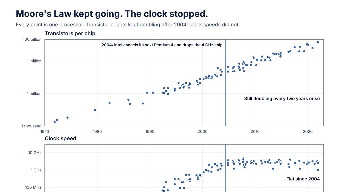
Between 1993 and 2004, the clock speed of Intel’s fastest PC processor went up almost sixty times. In the twenty years since, it has gone up less than twice. Ask most people why and they say Moore’s Law ended. It didn’t. Chips kept getting more transistors for years afterward. What ended was something quieter, with a less famous name: Dennard scaling.
That difference explains why every computer you’ve bought since 2005 has more cores instead of a faster clock, and why the chips that run AI today are judged by how fast they move data, not how fast they do math.
When the clock stopped, the industry was left with one way to turn transistors into speed: do more things at once. And once you are doing many things at once, the thing that limits you is the one from the first post in this series: the trip to memory.
One company saw this earlier than almost anyone and bet its processor roadmap on it. It was right about the architecture. It lost anyway. That pattern is worth understanding, because it is playing out again right now in AI chips.
Moore’s Law kept going, the clock stopped: transistors per chip and clock speed, one point per processor, about 100 processors, 1971 to 2021
Two laws, and only one of them died
Moore’s Law is about economics: the number of transistors you can put on a chip at a reasonable cost doubles roughly every two years. That kept going well past 2004.
Dennard scaling is about physics. In 1974, Robert Dennard and his colleagues at IBM published a paper in the IEEE Journal of Solid-State Circuits showing how to shrink a transistor and keep it well-behaved. The recipe, simplified: shrink every dimension of the transistor by some factor, and lower the voltage by the same factor, so the electrical stress inside the device stays the same.
Follow that recipe and several very pleasant things happen at once. Here it is for one typical generation, where everything shrinks to 0.7 of its old size:
Read the last line twice. Twice the transistors, each one faster, and the chip runs no hotter. The industry lived on that deal for thirty years. Moore’s Law gave you more transistors; Dennard scaling made them faster without costing more power. Herb Sutter would later call it the “free lunch”: wait a year and a half, and your software runs faster without you changing a line. People confuse the two laws because for three decades they always arrived together.
The recipe has a hidden assumption: you can keep lowering the voltage. You can’t, forever.
A transistor is a switch, and it flips at a threshold voltage. Lower the supply voltage and you have to lower the threshold too, or the switch can’t turn on hard enough to be fast. But lower the threshold and the switch no longer turns off cleanly. Current leaks through it even when it’s supposed to be off. Past a certain point that leakage becomes a large share of the chip’s power. Meanwhile the insulating layer in each transistor had become so thin that current tunneled straight through it.
The clearest statement of the problem comes from Dennard himself. In a 2006 IBM research report, he and his co-authors wrote that “transistor off current now limits further scaling of the threshold voltage.” A 2005 paper by Mark Horowitz and colleagues at Stanford, Intel and IBM put dates on it: from the 130-nanometer manufacturing generation onward, supply voltage “has been scaling slowly, if at all,” and in high-performance processors it had slowed even earlier, at 180 nanometers. The 180-nanometer generation reached the market around 2000, the 130-nanometer one around 2002.
So the voltage stopped falling while transistors kept shrinking. Take the voltage line out of that table and the arithmetic turns against you: twice the transistors, switching faster, now means more heat from every square millimeter, every generation. Horowitz’s paper summed it up: power had become “the number one problem in modern chip design.”
The physics broke gradually around 2000. The industry hit the wall in public in 2004:
May 2004. Intel cancelled Tejas and Jayhawk, the planned successors to the Pentium 4 and Xeon. The current Pentium 4, Prescott, already drew more power than the chip it replaced. Intel had already said publicly that its future was multi-core.
Fall 2004. Intel abandoned its plan to ship a 4 GHz Pentium 4. The 3.8 GHz Pentium 4 570J, released that November, was as fast as the line ever got.
March 2005. Herb Sutter’s essay “The Free Lunch Is Over” ran in Dr. Dobb’s Journal under the title “A Fundamental Turn Toward Concurrency in Software.” His verdict: “the clock race really is over, at least for now,” because of heat, power consumption and current leakage.
The numbers behind the opening: the original Pentium launched in March 1993 at 66 MHz. Eleven years later the Pentium 4 reached 3.8 GHz, nearly sixty times faster. In March 2024 Intel launched what it called the fastest desktop processor in the world, rated at “up to 6.2 GHz,” which is about 1.6 times the 2004 figure. That is a peak speed for short bursts, not what the chip sustains.
That’s the day the clock stopped. Moore’s Law kept handing out transistors. There was simply no longer a free way to make them faster.
If you can’t make one core faster, you build more cores. In April 2005 both x86 vendors shipped dual-core processors: Intel on April 18 with the Pentium Extreme Edition 840, and AMD on April 21 with dual-core Opteron.
But more cores only help if two things are true. The software has to have enough independent work to keep them busy. And the cores have to be able to get to their data.
The second one is the trap, and it’s the thesis of this series. In Post 1, with a CPU cycle stretched to one second, a trip to main memory became a six-minute coffee break. IEEE Spectrum reported in 2005 that a trip to off-chip memory “may take hundreds or even thousands of clock cycles,” leaving processor pipelines idle “as much as 85 percent of the time.” Put two fast cores on a chip and they share the same road to memory. Doubling the compute doesn’t double the work done if both cores are stuck in the same traffic.
William Wulf and Sally McKee, whom Post 1 introduced, had named this a decade earlier. Their 1995 paper “Hitting the Memory Wall” pointed out that processor speed was improving faster than memory speed, and concluded that “we are going to hit a wall in the improvement of system performance unless something basic changes.” As long as clocks kept rising, the industry could keep postponing that wall. When clocks stopped rising, it was the only wall left.
So the real question in 2005 wasn’t “how many cores?” It was “what kind of core do you build when cores spend most of their time waiting for memory?”
Intel and AMD’s first answer was the cautious one: take the big, fast core they already had, built to run one program as quickly as possible, and put two on a chip. Poonacha Kongetira, a senior engineering manager at Sun and lead author of its Niagara design paper, said Intel’s chips were “first designed for a single thread.”
Sun’s answer was radical, and it had been in the works for nearly a decade.
In 1996, Stanford professor Kunle Olukotun and his students published “The Case for a Single-Chip Multiprocessor,” arguing that several simpler processor cores on one chip would beat one ever-more-complex core. That work became Stanford’s Hydra project. Olukotun then co-founded a startup, Afara Websystems, with Les Kohn and Fermi Wang, to build the idea as a SPARC chip. In 2002, after the 2001 recession and 9/11 dried up its funding, Sun bought Afara. The chip, code-named Niagara, was officially named the UltraSPARC T1 in November 2005, and the first servers built on it launched on December 6, 2005.
The design is worth spelling out, because every choice in it is a bet about memory:
Eight small, simple cores. Each runs a short six-stage pipeline that issues one instruction at a time, and each still carries the SPARC register windows whose cost Post 2 described. There’s none of the elaborate machinery a big core uses to find other work while it waits on memory.
Four hardware threads per core, 32 in total. When one thread stalls on memory, the core switches to another with no lost cycles. The wait still happens; the core just doesn’t sit idle through it.
A low clock. 1.0 to 1.2 GHz, about a third of the speed of Intel’s fastest desktop chip.
Bandwidth everywhere. A 3 MB cache shared by all cores, a crossbar connecting them, and four DDR2 memory channels.
About 72 watts. That was a little over the 60 watts the designers had aimed for, but well under the 95 to 120 watts typical of mainstream x86 server chips at the time.
The design paper in IEEE Micro (Kongetira, Aingaran and Olukotun, 2005) lays out the logic. Business server software, such as databases and web servers, gives a single core little to work on in parallel and misses its caches often, so “the combination of low available ILP and high cache-miss rates causes memory access time to limit performance.” (ILP, instruction-level parallelism, is the work a single core can overlap within one program.) But that same software has enormous numbers of independent tasks: thousands of separate web requests or database queries. So stop trying to make one task fast. Run many slow ones and let them cover for each other: “the parallel execution of many threads effectively hides memory latency.”
A dictum Olukotun quoted in IEEE Spectrum might be the best one-sentence summary of this whole series: “you can always buy bandwidth, but latency is fixed by the speed of light, and you can’t bribe God.”
Notice that Niagara isn’t trying to make memory faster. It accepts that the trip to memory is long and will stay long, and it rebuilds the processor so that waiting is cheap. Keep that idea in mind. It comes back in a very big way in Post 6.
Niagara was not the first chip with more than one core. IBM’s POWER4 put two cores on one chip in 2001, and Sun’s own UltraSPARC IV was dual-core in 2004. What Sun did first was ship a mainstream processor designed from the ground up around the memory wall: many simple multithreaded cores at a deliberately low clock, built for total throughput rather than single-program speed. Intel and AMD went multicore because they had to. Sun went there because it believed that was the right machine for the work.
In April 2004, a month before Intel cancelled Tejas, Sun cancelled the UltraSPARC V, its next conventional high-speed flagship, along with a planned dual-core chip called Gemini. The official reason was “to accelerate the development of next-generation Throughput Computing systems.” It came a week after Sun announced 3,300 job cuts and a quarterly loss of up to $810 million.
“Throughput computing” wasn’t new marketing. Marc Tremblay, an architect of the UltraSPARC I and II and later CTO of Sun’s microelectronics business, was already using the phrase in 2000 for Sun’s MAJC processor. In 2005 Tremblay and colleagues wrote in IEEE Micro that server processor cores “are often idle, waiting for data or instructions coming from distant memory locations,” and predicted that chips like this would “take over all computing segments.” Rock, a later design Tremblay helped shape that aimed for throughput and single-program speed, never shipped.
For the high end, where customers still needed fast individual processors, Sun turned to Fujitsu. On June 1, 2004, the two announced that Sun would sell servers built on Fujitsu’s SPARC64 chips from 2006, splitting the high cost of designing and making processors. Sun’s own chips would chase throughput; Fujitsu’s would carry the high end.
By mid-2004, Sun had bet on the memory wall ea
正文由 探How 从来源站点 RSS 同步,内容未经改写;遇到排版缺失或需要图片、视频时请以原文为准。