Extreme Environments Push Chips to Their Breaking Point
Chips that were once qualified against a limited set of operating conditions are now being designed for environments where multiple stresses hit at once. Radiation, thermal shock, vibration, pressure, noise, and cryogen…
以下正文同步自 Hacker News 最新,版权归原站所有,已转换为易读排版。
Chips that were once qualified against a limited set of operating conditions are now being designed for environments where multiple stresses hit at once. Radiation, thermal shock, vibration, pressure, noise, and cryogenic temperatures are colliding in applications ranging from orbital data centers and defense systems to particle physics, quantum computing, and advanced manufacturing.
That is changing how chips are designed and qualified. AI-enabled design tools, machine learning, and language models can explore more design options earlier, but virtual models still have to be checked against physical behavior. For extreme-environment electronics, the challenge is not just predicting failure modes, but reproducing enough of the real operating environment to trust the prediction.
Space is becoming one of the clearest pressure points. The growth of satellite constellations, orbital data centers, space probes, surface explorers, and military space systems is increasing demand for radiation-hardened designs, including at newer process nodes where performance and power benefits must be balanced against survivability. That demand is already showing up in the design ecosystem.
“We have seen a major uptick in activity for rad-hard fab processes, particularly in the new process nodes to support orbital data centers,” said Dana Neustadter, senior director of product management at Synopsys. “A lot of this is owing to the Golden Dome (multi-layered U.S. missile defense initiative). The next frontier for the next battlefield is space, and so you’re seeing the investment now accelerate, and we’re going to see a lot more rad-hard designs added.”
Beyond national security, governments and nations are competing for global leadership in emerging technologies.
For example, Pacific Northwest National Laboratory (PNNL) is working with Morgan State University, Northrop Grumman, and Project Omega on the DARPA-funded Rads to Watts program, which aims to convert Cold War-era radioactive decay into high-density nuclear micro-power radiovoltaic systems for extreme environments, including space, remote sensing, undersea infrastructure, and defense applications. [1]
Radioisotopes such as Strontium-90 will be converted directly into electricity to operate for decades without refueling or battery replacement. Researchers achieve this by combining ultra-thin semiconductor layers with high-energy, beta-emitting isotopes. Simulation, characterization, and survivability analysis are essential to ensure these systems can operate in harsh environments.
Meanwhile, the U.S. Department of Energy’s Fermi National Accelerator Laboratory is working with Siemens on a project titled Accelerating eXtreme Environment Specs-to-Silicon (AXESS) that uses LLMs and smaller surrogate models to speed up design exploration, then integrate and co-optimize all stages of chip development for quantum computing, fusion energy, and particle physics. [2]
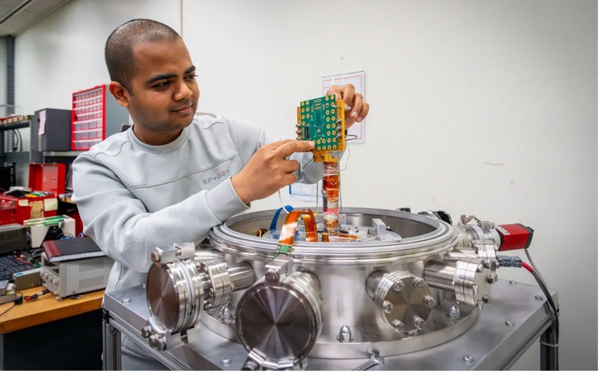
Fig. 1: A Fermilab engineer holds a custom circuit board designed to measure chip performance in cryogenic environments. Source: JJ Starr/Fermilab
Each extreme-environment application presents a unique set of physical stressors that the hardware device must account for.
“Particle accelerators and research accelerators are a particularly challenging environment because the doses are ridiculously high, and you need the equipment to do its thing while it’s getting damaged by the radiation,” said Hugh Barnaby, leader of extreme environment reliability in the U.S. Department of Defense’s ME Commons SWAP Hub at Arizona State University. “That extends to the medical equipment that’s used in proton therapies for cancer, which uses high-energy electrons. And in semiconductor manufacturing, lithography causes radiation damage. They’re using X-rays now for some of the really advanced technology, like backside power delivery. They have the power distribution on the backside of the chip. They used to use a wafer-analysis technique called LADA (laser-assisted device alteration), but now they can’t because the power is on the backside. They can’t use the lights. So they’re considering X-ray-assisted device alteration lasers (XADA). The problem is, they’re worried about the X-rays causing damage to the material.”
Barnaby and one of his students, Jereme Neuendank, found that strange things happen to semiconductors at very low temperatures. [3] “If you combine that with radiation, it gets even weirder,” said Barnaby. ” We had some good theories with models backing them up, and we’re still doing a lot of work in that area.”
Lab tools are evolving to study the effects of multiple stressors at once. ASU researchers developed the Rigel DSTAT, which has three rods collectively containing 9,000 Curies (Ci) of radioactive material to simulate the radiation environments found in space and nuclear applications. It also contains a tiny cryostat, which enables devices to be exposed to really saturated, extremely cold temperatures by evacuating a chamber and then filling it with either liquid nitrogen or argon, whose temperatures are about the same. “Then we can do radiation testing at liquid nitrogen, which is 77 Kelvin,” said Barnaby.
Fig. 2: This illustrated setup shows how ASU’s extreme environments lab would test radiation and extreme cold together to mimic space. Illustration by Sophia Franz. Source: ASU
The tool was ideal for a company designing readout ICs for satellites that would need to withstand cold, radiation, ionizing-dose threats, and low-frequency noise. In particular, random telegraph noise has emerged as one of the biggest reliability problems today, especially in analog/mixed-signal electronics. And that noise problem is exacerbated in the cold.
“You want the cold to reduce the noise that comes off of the diodes that are creating the currents, the light detectors,” Barnaby noted. “They like the cold there. But when you’re doing the CMOS, to do the readout of those signals, the random telegraph noise signal does not, at best, improve with cold temperature. We’re still studying that physics.”
The applications for these kinds of lab tools are growing. “We have talked to people about doing research in thermal energy exploration,” he explained. “We’ve also been getting into advanced packaging, which means extending into a pretty wide array of reliability issues such as pressure, humidity, high temperature — not just low — as well as radiation, thermal shock, mechanical shock, and vibration. We’re working with NXP quite a bit these days at their facility in Phoenix.”
Simulating electronics for space
Extreme environments such as space benefit from a 4D geospatial model and digital twin, which can include thermal and radiation data.
“If something gets hot, we can tell you how much the component stretches or shrinks or stresses,” said Shawn Carpenter, program director for 5G/6G and space at Synopsys, who recently worked with NASA on lunar network propagation. [4] “You can see whether the materials align and work properly. Thermal is a really big one for us because of the extremes that equipment goes through from direct illumination to shadow from the sun.”
Another stressor is that, in outer space, thermal cycling can range from -40°F to 120°F in the same day. “Your mean time to first failure is much higher,” said Lang Lin, director of product management at Synopsys. “We want to keep temperatures down because we want a very long lifetime for the electronics. But in outer space, when you have this thermal cycling changing so fast, it decreases the lifetime.” Then you add radiation. “All of our transistors here on Earth have a certain limited tolerance to radiation. But when you go to outer space, all the neutrons and protons and electrons from the sun go into the oxide of the transistors, and that messes up their performance.”
Designers need to build chips that support the particular mission. “We try to shorten the time it takes for someone to build a very capable chipset by providing them with IP for whatever target,” said Carpenter. “For example, the smaller nodes are highly desirable for the power that they’re going to save. We need to model the physics of that chip in operation. How hot does it get? Does it maintain signal integrity? How does it age? How long will it last? Will signals bleed into other parts of the package? Then there are integration questions. If I put that chip in a package, how does it perform? If I put that package on a carrier board, how does that perform? If I put it inside of a module, how do I get the heat out? How can I conduct that heat effectively? What are my power requirements?”
Simulation tools can answer all of those questions quickly. “If suddenly TSMC comes out with a 1.5nm process and you say, ‘Okay, I’m going to save 30% power by going to that new node, let’s go get the blocks, let’s re-spin the chip, let’s rebuild this stuff before we go out for the next mission,’ then we build that out to the system evaluation,” he said. “How does the chip work, as informed by where you’re operating it, how you’re using it, and the cycles it’s going to go through for heating and whatever else the environment throws at it?”
For space applications, physics questions need to be answered in the context of a large, gravitationally informed environment where things swirl at incredible speeds.
Simulation, digital twinning, and AI-enabled tools can be combined to model objects, people, and systems in orbit or on the lunar surface. “You don’t want that data spoofed, so that the location is actually different than what you think it is,” Neustadter warned.
Agentic AI will also be part of the equation. “Especially when you start talking about militaristic functionality — vehicles that are going to be more like a drone, in the use case of an orbital communications hub or orbital lab, these vehicles are going to need to be mobile, they’re going to need to react, they’re going to have weapon systems on them,” said Neustadter. “We know there are nuclear warheads already up there, and that’s part of how we destroy or circumvent them.”
AI doesn’t always enhance safety, but it increases adaptability. Neustadter noted that if you lose control of a vehicle, it should be autonomous most of the time and able to learn and transmit data. Since communication costs are high at the desired data rates, it’s beneficial to handle some processing locally and only send the critical information back.
Counteracting radiation
Many military components already are prepared for a nuclear event in space, which disrupts the electromagnetic pulses (EMP) of all the electronics.
“The military has to have protection against EMP and high-altitude EMP (HEMP),” said Lin. “Military airplanes require extremely expensive shielding and grounding techniques that are not required for commercial aviation and some of the electronics we have today. But for space applications, that’s required, and it’s more expensive. DO-160 EMC certification requirements are more for aerospace. Whenever you have an EMP, and that could be because of a nuclear reaction or sun storms, you have a potential issue with your electronics. If the electronics aren’t strong enough, the EMP will generate some inrush current, and you’re going to have to reset your computer.”
After a reset, EMP-induced excess current can damage semiconductors. “Then you’re going to have to replace it,” Lin said. “It depends on the EMP level and the protection needed. Currently, no data centers here on Earth have EMP protection, but space-based ones will likely need specialized shielding, which would raise development costs for orbital data centers.
On Earth, AI data centers and automotive systems need less protection from atmospheric radiation than in space, but single event upsets caused by unusual sun activity and cosmic rays are still a concern.
“Cosmic rays cause bit flips and other random events, which can be catastrophic for the AI training ru
正文由 探How 从来源站点 RSS 同步,内容未经改写;遇到排版缺失或需要图片、视频时请以原文为准。